
Trapping Phenomena in Nanocrystalline Semiconductors
Non-equilibrium free carriers (electrons and holes) can be generated in bulk semiconductor materials by various processes, such as light absorption, high electric field, carrier injection through a barrier, irradiation with high-energy particles. After the process which has generated the non-equilibrium carriers has ceased, the system returns to equilibrium due to the annihilation of the electron-hole pairs by recombination. If the carriers that recombine are both free (the electron in the conduction band and the hole in the valence band), their annihilation process is called band-to-band recombination. If one of the carriers is captured on a localized state (i.e., it has a fixed position in the semiconductor) and the other one is free, this is called recombination on localized states.
By the recombination process, an amount of energy is released by the emission of either a photon (radiative recombination), or a phonon (non-radiative recombination), or a secondary electron (Auger recombination), etc. A carrier captured on a localized state can recombine with an opposite sign carrier, if this opposite sign carrier is subsequently captured on the same localized state, or it can be released in the corresponding band (conduction band for electrons and valence band for holes). The capture of a second carrier with an opposite sign on the same localized state leads to the annihilation of the pair and it is called recombination on a localized state. If the captured carrier is released in the band, the capture center is called a trap. Then the capture process is called trapping and the release process is called detrapping. These different situations are presented in Fig. 1.
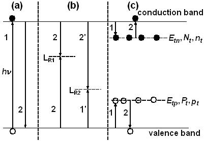
Fig. 1. Transitions in bulk semiconductors:
(a) intrinsic absorption and band-to-band recombination;
(b) recombination levels; (c) trapping levels.
The traps can be classified based on different criteria. Following the trapped charge, there are two kinds of traps: traps for electrons and traps for holes. Following the location, there are also two kinds of traps: bulk traps and surface/interface traps. The impurities, point defects, surface states, dangling bonds, and also localized stresses can act as trapping centers. The trapping levels are usually located in the band gap, but they can also exist in the conduction or in the valence band. In bulk semiconductors, trapping phenomena are dominated by the traps located in the volume of the crystals, such as point defects, impurities, and local stresses.
At the same time, in nanocrystals these phenomena are dominated by the traps located at the surface/interface. The latter is due to the very large surface/volume ratio (of the order of 106 cm-1). Therefore, the number of atoms located at the surface/interface is of the same order of magnitude as the total number of atoms. Any such atom can act like a trap or recombination center, so that the surface/interface of a nanosystem plays a major role in the non-equilibrium processes. Most of the surface/interface traps are adsorbed atoms/molecules, dangling bonds, or misfit-induced internal stresses.
In nanowires and nanolayers, one finds the same kinds of traps as in bulk semiconductors. In nanodots, a supplementary capture phenomenon appears on the quantum confinement (QC) levels. The carriers captured this way are not localized at atomic scale, like the “classical” traps, but at nanodot scale (i.e., they can move inside the nanodot only). Thus, for “small” nanodots (usually called “quantum dots”), with diameters less than the order of magnitude of 10 interatomic distances, this localization is strong enough to play a significant role in the trapping-detrapping processes and/or the recombination on localized states. A specific characteristic of a quantum dot is that it has no real energy bands and no momentum conservation. This is due to the small number of atoms that can be found in any direction.
At the same time, the QC introduces supplementary levels, as the quantum dot surface acts like the wall of a quantum well. These levels are located over the last occupied level at absolute zero temperature (i.e., between the quasi-valence and the quasi-conduction bands). There are two ways to make such levels act like traps. One way is to inject a carrier into a quantum dot by tunneling (there is no other way to make a carrier enter or leave a quantum dot, as its surface acts like a barrier). This supplementary carrier cannot recombine with an opposite sign carrier, as there are no real energy bands in a quantum dot to act like carrier reservoirs. The carrier remains trapped until it leaves the quantum dot or recombines with an opposite sign carrier subsequently injected in the quantum dot. Another way to produce a non-equilibrium carrier is to excite an electron from a lower state into a higher one (producing at the same time a hole in the initial state). If the tunneling probabilities of the electron and hole are different, one of them leaves the quantum dot and then both will act like non-equilibrium carriers trapped in different dots.
The behavior of carriers in quantum dots also depends on their Coulomb interactions. The Coulomb repulsion between two equal charges inside a quantum dot becomes so important that it does not allow the simultaneous presence of more than one non-compensated charge in the quantum dot. This phenomenon is called “Coulomb blockade”. Therefore, if several trapping centers for the same sign carriers are located in the same quantum dot, only one of them could be occupied. If traps of both signs are located in the same quantum dot, special complications could arise. Let us discuss the case of three trapping centers located in the same quantum dot, with the activation energies ΔEt1, ΔEt2, and ΔEt3 (by convention, ΔEt1 ≤ ΔEt2 ≤ ΔEt3). What happens if we try to charge all of them? If the first two centers (ΔEt1 and ΔEt2) are traps for the same sign carriers, they cannot be simultaneously charged, whatever charge could be trapped on the third center. If the first two centers trap opposite sign carriers, all three centers can be charged simultaneously.
The discharge of the traps is also dependent on the charge signs. If the first and third centers trap charges with the same sign, the discharge of the three levels will happen in normal order, i.e., one by one, starting with the lowest energy. If the second and third centers trap charges with the same sign (opposite to the first center, see Fig. 2a), the discharge of the first level would imply the double charging of the quantum dot, which is forbidden by the Coulomb blockade (Fig. 2b). Consequently, the second level will be discharged simultaneously with the first one (Fig. 2c). This means that the experimental measurements will lead to the observation of a single experimental maximum corresponding to the first two levels, with the apparent activation energy ΔEt ≈ (ΔEt1 + ΔEt2)/2. Meanwhile, the discharge of the third level will produce a “normal” maximum, with the real activation energy ΔEt3.
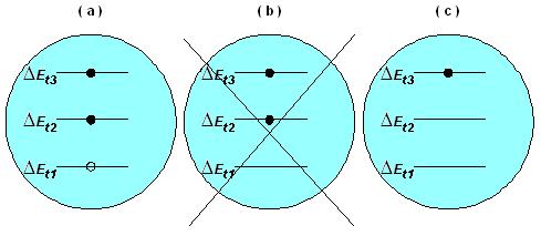
Fig. 2. The trapping-detrapping process in a quantum dot with three centers. (a) All traps are charged; (b) the lowest energy level cannot be discharged solely, due to the Coulomb blockade effect; (c) simultaneous discharge of the lowest two energy levels.
The conventional experimental methods most frequently used for the investigation of traps, based on the exponential decay transience, the rate window approach and the thermally stimulated behavior, are described. These methods are:
- - the deep level transient spectroscopy (DLTS), with its constant capacitance voltage transient (CCVT) variant;
- - the photoinduced current transient spectroscopy (PICTS);
- - the thermally stimulated currents (TSC) method and its adaptations - the thermally stimulated depolarization currents (TSDC) and the optical charging spectroscopy (OCS) methods.
All these methods are discussed with respect to their suitability for the trap investigation in nanocrystalline semiconductors and to the trap parameters that can thus be obtained. Most of the conventional methods used for the trap investigation in bulk semiconductors (like PICTS, TSC, TSDC, and OCS) are also applied to the nanocrystalline ones. For instance, the OCS method is a very sensitive one because the discharge current is a superlinear function of the trap concentrations. A thorough modeling allows the determination of trap parameters that are not directly measurable. However, some of the conventional methods (like DLTS) are not very suitable for nanocrystals.
The application of these methods, together with different non-conventional methods, to the study of the traps in nanocrystalline semiconductors, is presented. Among the non-conventional methods there are:
- - the use of an atomic force microscope (AFM) to charge the traps and then image them;
- - the study of the Coulomb blockade spectrum of a nanodot prepared for a single electron transistor;
- - the spin-dependent recombination (SDR) method (measuring C–V or R–V characteristics in an electron spin resonance device);
- - the use of a low-energy electron point source (LEEPS) microscope to image the shadow of a carbon nanotube on an electron detector;
- - the analyze of the time-of-flight (TOF) in transient photocurrent;
- - the study of the single nanodot photoluminescence (PL) intensity fluctuations (blinking);
- - the study of the thermoluminescence (TL).
For instance, the SDR method determines the deep trap energies and presents the advantage to identify their nature, by means of the hyperfine interactions. The TOF technique for transient photocurrent measurements also allows the estimation of the trap energy and concentration. On the other hand, the AFM and LEEPS microscopes permit the observation and the mapping of individual charged traps. Different investigation methods are complementary to each other and therefore ought to be used together to obtain full information about the traps.
The investigation of the trapping-detrapping phenomena in semiconductor materials and devices is essential for several processes. In the case of nanocrystalline semiconductors, specific effects appear. In the electrical transport through a quantum dot system, the current is reduced by the trapping of the carriers inside the quantum dots. In the case of the phototransport, the trapping of one type of carrier (electrons or holes) increases the lifetime of the opposite sign carriers and thus the recombination rate decreases. Therefore the photocurrent increases. Light absorption is always increased by the presence of the traps, while light emission depends on the radiative versus non-radiative contributions. It is important to know both how to use the traps beneficially whenever possible and how to minimize the problems they can create.
There are several specific applications of the traps. For example, in NROM (Nitride Read Only Memory) non-volatile memory cells, the traps in the silicon nitride (Si3N4) nanolayer are used for charge storage. Also, the traps at the surface/interface of silicon nanodots are proposed for application in the memory devices. On the other hand, traps can induce a reduction of the device reliability. For example, in the case of thin SiO2 gates, the traps contribute to the wear out of the oxide through the weakening of the Si-O bond by the trapped electrons. The study of p-channel MOSFETs proved that the application of a moderate temperature stress at negative bias induces a significant increase in interface trap concentration, which in turn produces an increase in the temperature instability of the transistor at a negative bias.
The role of the traps in electrical processes was investigated mainly for the group IV semiconductors. As an example, the gate leakage current in MOSFETs is influenced by the traps located in the gate oxide or at its interface with the substrate. The trapped electrons contribute to the wear out of the oxide through the weakening of the Si-O bond. This leads to quasi-breakdowns (or soft breakdowns), i.e., the rather abrupt increase of the leakage current, reducing the reliability. The trap concentration is strongly increased by the presence of nanodots into the oxide. More than that, almost all the charge is stored on the nanodots if they are located at the edge of the oxide. If the nanodots are coated, the core/shell interface traps will act as a long-term electrical memory.
At the same time, the apparent mobility of the carriers through the channel of a high k MOSFET is sensibly reduced by the presence of traps in the dielectric. This is due to the increase in the effective threshold voltage and the decrease in the drain current, both induced by the charge accumulation in the traps located in the dielectric. On the other hand, the traps located in the vicinity of a nanodot influence its behavior by means of electrostatic interactions. Thus, the Coulomb blockade oscillations of the source-drain conductance in a single electron transistor are intensely modulated in amplitude and phase by the traps located near the nanodot. This can drastically affect the transistor behavior.
The trap contributions to the optical processes were studied mainly for II-VI and III-V semiconductors. The requirement of bright PL nanodots for biological markers and optoelectronic devices implies the healing of the surface traps. The passivation of the nanodot surface (CdSe, CdS, or InAs), either by capping or coating, proved itself a very good healing method. At the same time, the shifts of the absorption and PL peaks for the coated dots could be related with the shift of the QC levels due to the diameter increase. A specific phenomenon for the II-VI nanodots, the blinking PL of a single nanodot, has been explained by the modeling of the oscillation of the carriers between the QC levels in a nanodot and the surface traps. On the other hand, the trapping on QC levels allows an efficient electroluminescence of Si nanodots subjected to an a.c. bias. This allowed the fabrication of a light source from a floating gate MOSFET, by inserting an array of quantum dots in the oxide layer.
The small number of atoms in a nanocrystalline semiconductor makes the contributions of the traps to different phenomena much more important than in bulk semiconductors. The trapping phenomena can be used to produce different devices, like floating gate memories, light-emitting transistors, and biological markers. On the other hand, the traps can reduce the reliability of the electronic devices and perturb their functioning. Therefore, their study is a stringent necessity.
Acknowledgement
This web page was created by Magdalena Lidia Ciurea, head of the laboratory of low dimensional systems, National Institute of Materials Physics, Bucharest, Romania. The page is a brief summary of the chapter 8 from the book Nanoelectronics and Photonics: From Atoms to Materials, Devices and Architectures (published with permission from Springer)