
Semiconductors
Semiconductor Structure
Semiconductors are made up of individual atoms bonded together in a regular, periodic structure to form an arrangement whereby each atom is surrounded by 8 electrons. An individual atom consists of a nucleus made up of a core of protons (positively charged particles) and neutrons (particles having no charge) surrounded by electrons. The number of electrons and protons is equal, such that the atom is overall electrically neutral. The electrons occupy certain energy levels, based on the number of electrons in the atom, which is different for each element in the periodic table. The structure of a semiconductor is shown in the figure below.
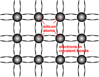
Schematic representation of covalent bonds in a silicon crystal lattice.
The atoms in a semiconductor are materials from either group IV of the periodic table, or from a combination of group III and group V (called III-V semiconductors), or of combinations from group II and group VI (called II-VI semiconductors). Silicon is the most commonly used semiconductor material as it forms the basis for integrated circuit (IC) chips. Most solar cells are also silicon based. Several properties of silicon are described at the silicon page.
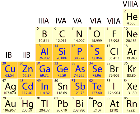
Section from the periodic table. More common semiconductor materials are shown in blue. A semiconductor can be either of a single element, such as Si or Ge, a compound, such as GaAs, InP or CdTe, or an alloy, such as SixGe(1-x) or AlxGa(1-x)As, where x is the fraction of the particular element and ranges from 0 to 1.
The bond structure of a semiconductor determines the material properties of a semiconductor. One key effect is limit the energy levels which the electrons can occupy and how they move about the crystal lattice. The electrons surrounding each atom in a semiconductor are part of a covalent bond. A covalent bond consists of two atoms "sharing" a single electron, such that each atom is surrounded by 8 electrons. The electrons in the covalent bond are held in place by this bond and hence they are localised to region surrounding the atom. Since they cannot move or change their energy, electrons in a bond are not considered "free" and cannot participate in current flow, absorption or other physical processes which require presence of free electrons.
However, only at absolute zero are all electrons in a bonded arrangement. At elevated temperatures, the electron can gain enough energy to escape from its bond, and if this happens, the electron is free to move about the crystal lattice and participate in conduction. At room temperature, a semiconductor has enough free electrons to allow it to conduct current, while at, or close to absolute temperatures, a semiconductor behaves like an insulator.
The presence of the bond introduces two distinct energy states for the electrons. The lowest energy position for the electron is to be in its bound state. However, if the electron has enough thermal energy to break free of its bond, then it becomes free. The electron cannot attain energy values intermediate to these two levels; it is either at a low energy position in the bond, or it has gained enough energy to break free and therefore has a certain minimum energy. This minimum energy is called the band gap of a semiconductor. The number and energy of the free electrons is basic to the operation of electronic devices.
The space left behind by the electrons allows a covalent bond to move from one electron to another, thus appearing to be a positive charge moving through the crystal lattice. This empty space is commonly called a "hole", and is similar to an electron, but with a positive charge.
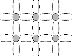
Animation showing formation of "free" electrons and holes when an electron can escape its bond.
The most important parameters of a semiconductor material for its operation in electronic devices and solar cells are:
- - the band gap;
- - the number of free carriers available for conduction; and
- - the "generation" and recombination of free carriers in response to the electric field, temperature and light shining on the material.
More detail on these properties is given in the following pages.
Band Gap
 The band gap of a semiconductor is the minimum energy required to move an electron from its bound state to a free state where it can participate in conduction. The band structure of a semiconductor gives the energy of the electrons on the y-axis and is called a "band diagram". The lower energy level of a semiconductor is called the "valence band" (EV) and the energy level at which an electron can be considered free is called the "conduction band" (EC). The band gap (EG) is the distance between the conduction band and valence band.
Once the electron is in the conduction band, it is free to move about the semiconductor and participate in conduction. However, the movement of an electron to the conduction band will also allow an additional conduction process to take place. The movement of an electron to the conduction band leaves behind an empty space for an electron. An electron from a neighboring atom can move into this empty space. When this electron moves, it leaves behind another space. The continual movement of the space for an electron, called a "hole", can be illustrated as the movement of a positively charged particle through the crystal structure. Consequently, the movement of an electron to the conduction band gives results in not only an electron in the conduction but also a hole in the valence band. Both the electron and hole can can participate in conduction and are called "carriers".
The concept of a moving "hole" is analogous to that of a bubble in a liquid. Although it is actually the liquid that moves, it is easier to describe the motion of the bubble going in the opposite direction.
Intrinsic Carrier Concentration
The thermal excitation of a carrier from the valence band to the conduction band creates free carriers in both bands. The concentration of these carriers is called the intrinsic carrier concentration, denoted by ni. Semiconductor material which has not had impurities added to it in order to change the carrier concentrations is called intrinsic material. The intrinsic carrier concentration is the number of electrons in the conduction band or the number of holes in the valence band in intrinsic material. This number of carriers depends on the band gap of the material and on the temperature of the material. A large band gap will make it more difficult for a carrier to be thermally excited across the band gap, and therefore the intrinsic carrier concentration is lower in higher band gap materials. Alternatively, increasing the temperature makes it more likely that an electron will be excited into the conduction band, which will increase the intrinsic carrier concentration.
Intrinsic Carrier Concentration of Silicon as a Function of Temperature
At 300 K the generally accepted value for the intrinsic carrier concentration of silicon, ni, is 1.01 x 1010 cm -3 (Sproul). The previously accepted value was 1.45 x 10¹⁰. An empirical fit to the measured data over the range 275 K to 375 K is given by:
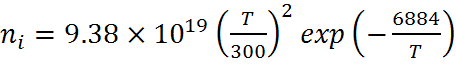
While the intrinsic carrier concentration is normally quoted at 300 K, solar cells are usually measured at 25 °C where the intrinsic carrier concentration is 8.6 x 109 cm -3
Doping
It is possible to shift the balance of electrons and holes in a silicon crystal lattice by "doping" it with other atoms. Atoms with one more valence electron than silicon are used to produce "n-type" semiconductor material, which adds electrons to the conduction band and hence increases the number of electrons. Atoms with one less valence electron result in "p-type" material. In p-type material, the number of electrons trapped in bonds is higher, thus effectively increasing the number of holes. In doped material, there is always more of one type of carrier than the other and the type of carrier with the higher concentration is called a "majority carrier", while the lower concentration carrier is called a "minority carrier."
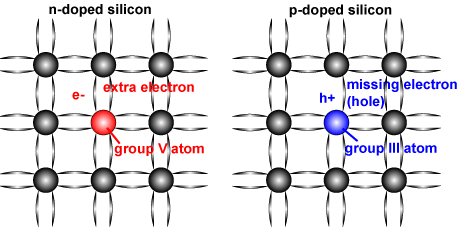
The following table summarizes the properties of semiconductor types.
| P-type (positive) | N-type (negative) | |
|---|---|---|
| Dopant | Group III (E.g. Boron) | Group V (e.g. Phosphorous) |
| Bonds | Missing Electrons (Holes) | Excess Electrons |
| Majority Carriers | Holes | Electrons |
| Minority Carriers | Electrons | Holes |
In a typical semiconductor there might be 1017cm-3 majority carriers and 106cm-3 minority carriers. Expressed in a different form, the ratio of minority to majority carriers is less than one person to the entire population of the planet. Minority carriers are created either thermally or by incident photons.
Equilibrium Carrier Concentration
The number of carriers in the conduction and valence band with no externally applied bias is called the equilibrium carrier concentration. For majority carriers, the equilibrium carrier concentration is equal to the intrinsic carrier concentration plus the number of free carriers added by doping the semiconductor. Under most conditions, the doping of the semiconductor is several orders of magnitude greater than the intrinsic carrier concentration, such that the number of majority carriers is approximately equal to the doping.
At equilibrium, the product of the majority and minority carrier concentration is a constant, and this is mathematically expressed by the Law of Mass Action.
where ni is the intrinsic carrier concentration and n0 and p0 are the electron and hole equilibrium carrier concentrations.
Using the Law of Mass Action above, the majority and minority carrier concentrations are given as:
| n-type: |  , , |
 |
|---|
| p-type: |  , , |
 |
|---|
The above equations show that the number of minority carriers decreases as the doping level is increases. For example, in n-type material, some of the extra electrons added by doping the material will occupy the empty spots (i.e, holes) in the valance band, thus lowering the number of holes.
Acknowledgement


This web page is an adapted version of the article at the PVCDROM web site (with permission from the authors Stuart Bowden and Christiana Honsberg).
More about semiconductors
- Principles of Semiconductor Devices by Bart van Zeghbroeck, University of Colorado
- Semiconductor Tutorial by N. Cheung, U.C. Berkeley
- Semiconductors by Tony Kuphaldt, chapter III, on-line books series at allaboutcircuits.com
- Electrical Engineering Training Series from Integrated Publishing
- Semiconductor Lectures by R.C. Word, Portland State University
- Britney Spears Guide To Semiconductor Physics