
Photovoltaic Thin Film Solar Cells
Photovoltaic Effect
When a photovoltaic (PV) cell is exposed to sunlight, voltage and electric current are created in the cell. This process is based on the photoelectric effect in which light is absorbed and excites an electron to a higher energy level. The main difference between the so called photoelectric effect and photovoltaic effect is that in the first case, the excited electron is bounced out of the material while in the second process it is still contained inside the material. However, in both cases, an electric potential is produced related to separation of charge carriers. Hence, to prevail the created potential barrier, the incident light should have enough energy. The figure below shows the both photoelectric effect and photovoltaic process schematically.
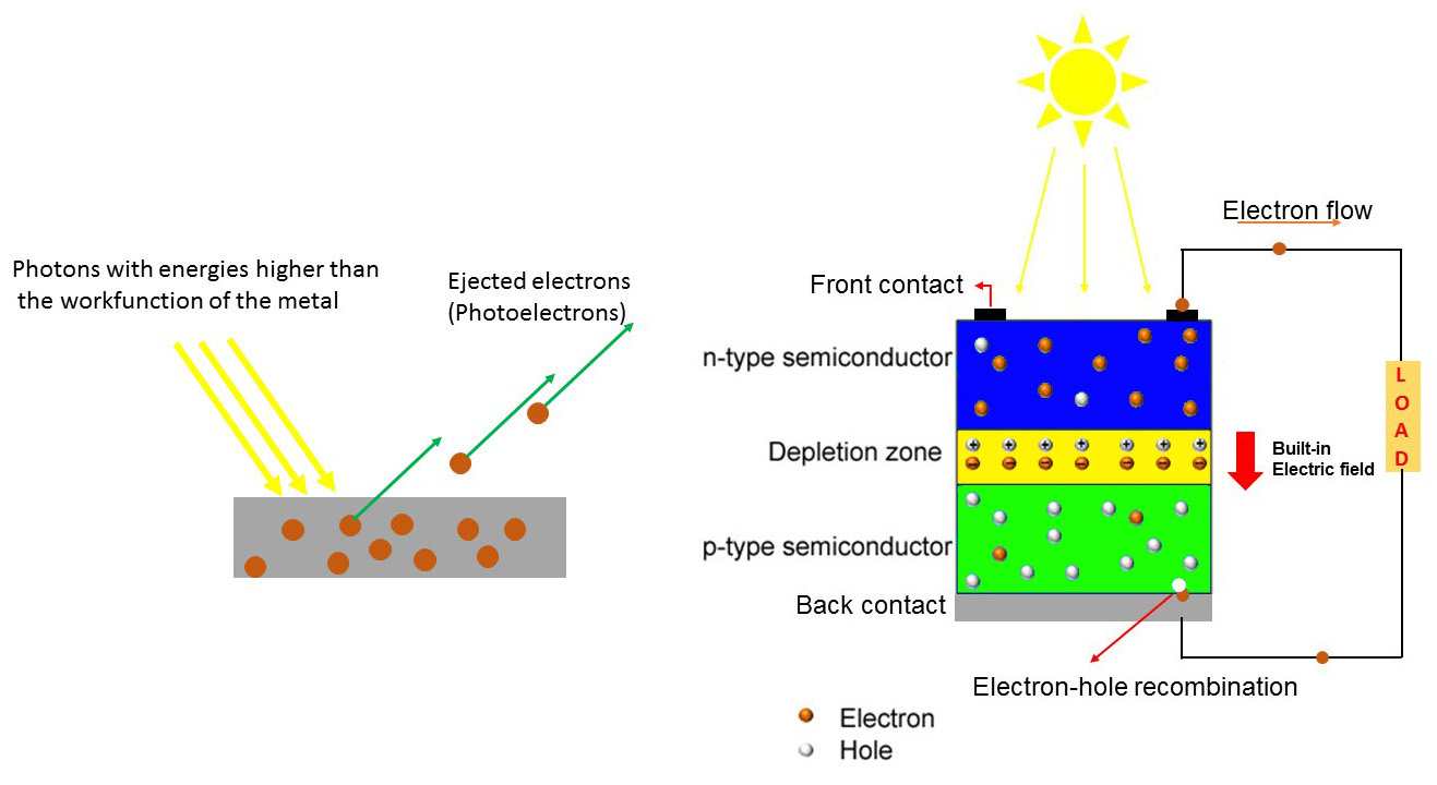
Schematic representation of what happens in photoelectric effect (left) and in a PV solar cell (right).
In a PV solar cell, a p-type and a n-type semiconductor are placed in a physical contact with each other. Consequently, a narrow region is created between the junction of the materials. This region is called the depletion zone or the space charge region. Atoms in one side of this region are depleted of electrons (positively charged ions) and in the other side are depleted of holes (negatively charged ions) resulting in an induced electric field (called built-in electric field). Hence, if a charged particle is placed in this region, it will move from one side of the region to the other side.
How a PV solar cell works
The question is that what happens when a solar cell operates under the sunlight? The photons coming from the sun can be considered as individual particles carrying a certain amount of linear momentum (p=h/λ, where h is the well-known Plank constant and λ stands for the light wavelength). The corresponding energy equals E=hc/λ where c is the speed of the light in free space. This amount of energy should be equal or greater than the energy bandgap of the semiconductor. Otherwise the incident light won’t be absorbed by the layer and the layer will be transparent for the light. In this case we are not interested in having a so wide bandgap semiconductor material to be assured that the majority of the incident light will be absorbed and contribute to generate the charge carriers. As it has been shown in the figure, the topmost layer of a PV solar cell is a n-type semiconductor (called the window layer). Photons enter from the window layer and excite electrons to the conduction band. Each ejected electron leaves a vacancy or a “hole” in the valence band. This process is called an electron-hole pair generation. The ejected electron and the corresponding left hole are still associated with each other and tend to recombine. If they are left alone without any applied field to make them moved, they will compensate. The mentioned excited electron-hole state is called an exciton. Remembering that the process started on the n-type side, the created exciton would travel on the direction of the p-n junction while reaches the depletion layer where an electric field (built in electric field that was explained above) has been established. The electric field separates the electron from the hole, and pushes them to opposite directions. Hence, a dc electric current is produced in the closed circuit. In a way that an electron's current flowing to one side of the circuit and a hole's current flowing to the opposite side.
Thin film solar cells
The philosophy of tendency toward thin film PV solar cells lies in the context of Shockley-Queisser limit (SQL) that calculates the maximum solar conversion efficiency around 33.7% for a single junction solar cell [1]. Thin film solar cells with multiple layers can overcome this limit. The main considerations that result in SQL include: blackbody radiation, recombination and spectrum losses.
Blackbody radiation
All materials will give off electromagnetic (EM) radiation at the temperatures higher than the absolute zero. As we know, a blackbody absorbs all incident EM radiation. This name is given because it doesn’t reflect the incident radiation but absorb all of it. It is seen black when it is cool at room temperature. At the same time, it is a perfect EM emitter and emits EM radiation that its spectrum is determined by temperature merely. About 7% of all amount of energy that is absorbed by a solar cell will be emitted through the blackbody radiation at room temperature (300 K). In the absence of solar irradiation, the solar cell and the ambient are in a thermodynamic equilibrium. On the other hand, solar irradiation, Joule heating and electron-hole recombination cause increase of the cell temperature. When the solar cell temperature increases the blackbody radiation increases too once the equilibrium is attained. Practically, the equilibrium is reached around 360 K (87˚C). The open circuit voltage (Voc) of a solar cell is the most sensitive parameter to the temperature and decreases as the temperature increases and the cell operate at lower efficiencies than its room temperature rating.
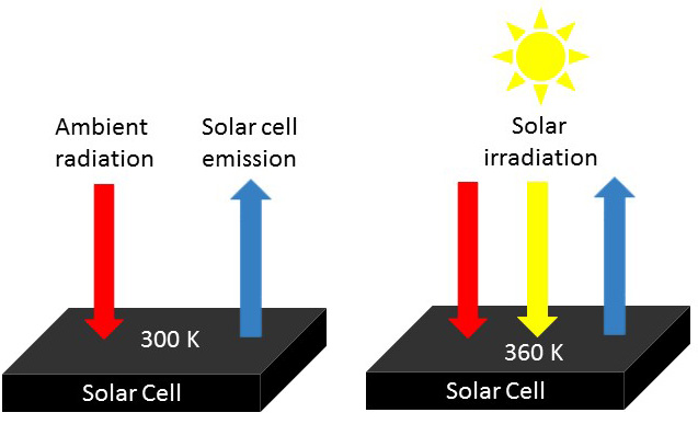
A solar cell emits approximately 7% of the absorbed energy through blackbody radiation at room temperature (300 K). The cell temperature increases when it is exposed to the sunlight and the equilibrium is reached at about 360 K.
Recombination
Absorption of photons with enough energy generates an electron-hole pair in a semiconductor material. In the absence of any electrical field, the created electron-hole pair will recombine in a reverse process. In the SQ model, the recombination rate is a function of the electrical potential across the cell. About 02% of energy is lost in a solar cell from the local recombination of newly created electron-hole pairs.
Spectral losses
Indeed, a solar cell can solely convert solar radiation to the electricity efficiently for photons with energies just above the bandgap value. In other words, photons with energies lower than the bandgap energy cannot contribute to the power production. This is one part of the spectral loss that takes place in a solar cell. For instance, the bandgap value of silicon is about 1.1eV that is corresponding to the IR light. Accordingly, radio waves, microwaves, and most infrared photons wont contribute to the power production. Another contribution of the mentioned spectral loss is related to the photons with much higher energies than the bandgap value (E>>Eg). At the first look it may seem that the blue light for instance that has approximately twice energy of red light will be well captured by a single junction solar cell. While, what is happening in reality is a bit different. For photon energies much higher than the bandgap, an electron will be ejected well above the band edge, but the extra energy will be converted into heat very rapidly (thermalization) as the ejected electron goes back to the band edge.
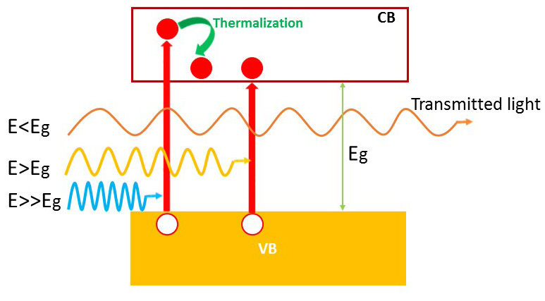
Photons with energies much higher than the bandgap (Eg) are jumped up deeply to the conduction band (CB) and then thermalized back to the band edge. Photons with energy just above the band edge are absorbed well and contribute to the power production. Photons with energies less than the bandgap won’t be absorbed and will travel freely across the semiconductor.
Regarding the abovementioned limiting factors, stacking up layers with desired electrical and optical properties can make an efficient thin film solar cell.
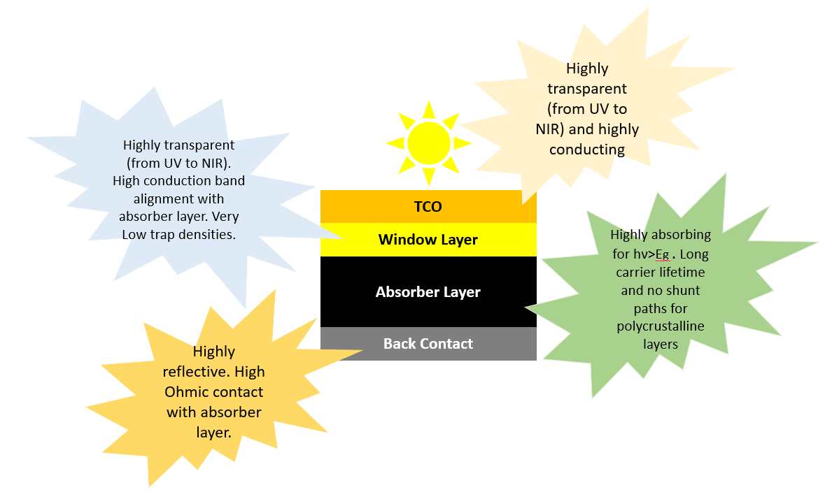
Schematic presentation of required electrical and optical properties of different layers of a typical PV thin film solar cell to produce high power.
Using an absorber layer with an optimum bandgap value is the most critical issue in PV solar cells. From SQL, there is a tradeoff between the number of the absorbable incident photons and the maximum energy taken per photon. Thin film solar cells provide the possibility of light management. To accomplish this, various p-n junctions each one tuned to a specific wavelength of solar spectrum are used. Generally, the upper layers are grown very thin so that they are transparent to lower frequencies (longer wavelengths). As a consequence, the stacked top layers capture the shortest wavelengths while the longer wavelengths pass through them and are absorbed by the lower layers.
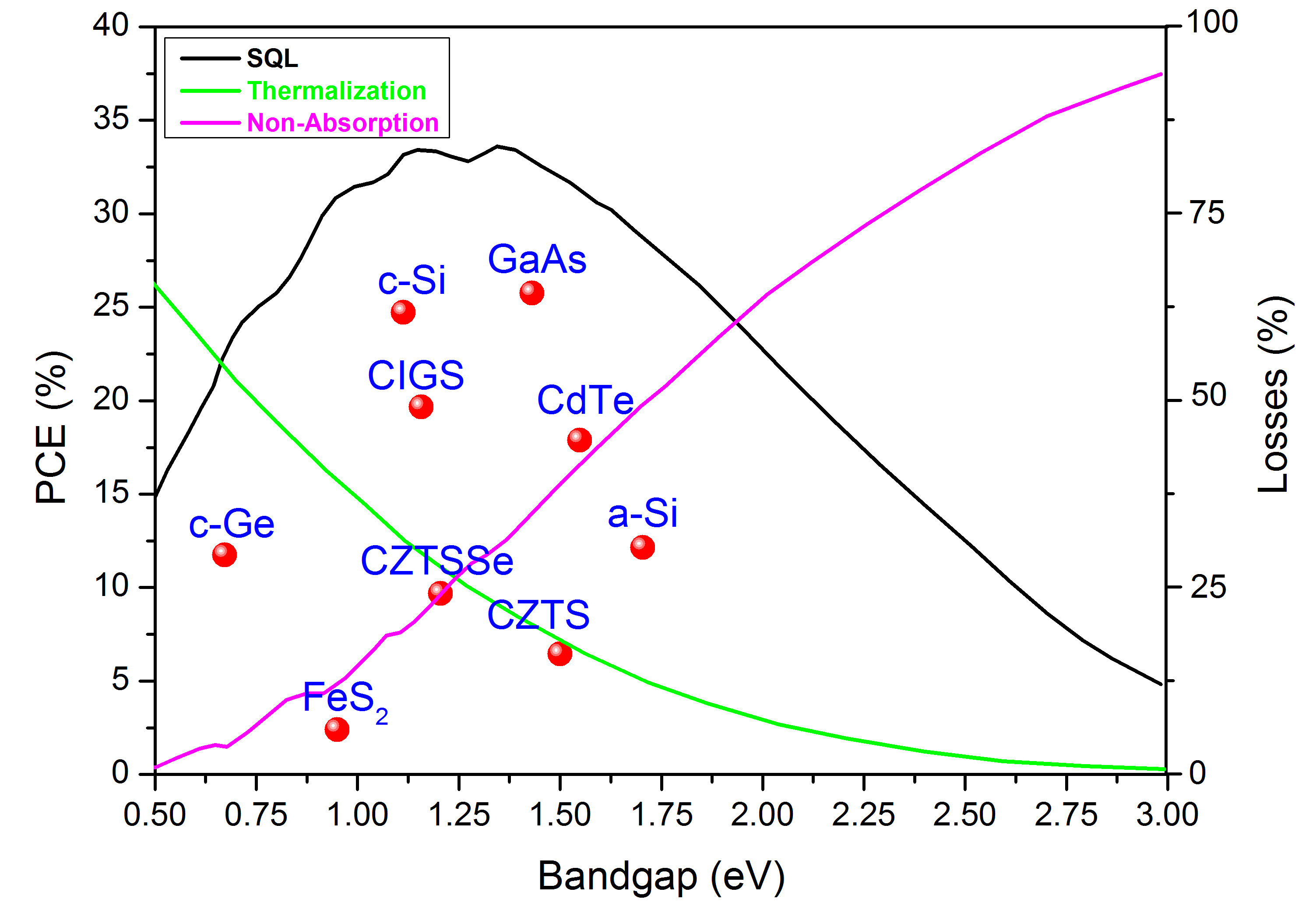
The reported maximum power conversion efficiencies (PCEs) of single-junction thin film solar cells under AM1.5 illumination versus bandgap values of a number of absorber layers along with the graphs showing the Shockly-Queisser limit (SQL) and losses due to thermalization and non-absorptive processes.
Acknowledgement

Content of the web page has been developed by Ali Abdolahzadeh Ziabari, Senior Research Scientists at Islamic Azad University Lahijan Branch.