
P-N Junctions
Formation of a P-n junction
P-n junctions are formed by joining n-type and p-type semiconductor materials, as shown below. Since the n-type region has a high electron concentration and the p-type a high hole concentration, electrons diffuse from the n-type side to the p-type side. Similarly, holes flow by diffusion from the p-type side to the n-type side. If the electrons and holes were not charged, this diffusion process would continue until the concentration of electrons and holes on the two sides were the same, as happens if two gasses come into contact with each other.
However, in a p-n junction, when the electrons and holes move to the other side of the junction, they leave behind exposed charges on dopant atom sites, which are fixed in the crystal lattice and are unable to move. On the n-type side, positive ion cores are exposed. On the p-type side, negative ion cores are exposed. An electric field Ê forms between the positive ion cores in the n-type material and negative ion cores in the p-type material. This region is called the depletion region since the electric field quickly sweeps free carriers out, hence the region is depleted of free carriers. A "built in" potential Vbi due to Ê is formed at the junction.
Carrier Movement in Equilibrium
A p-n junction with no external inputs represents an equilibrium between carrier generation, recombination, diffusion and drift in the presence of the electric field in the depletion region. Despite the presence of the electric field, which creates an impediment to the diffusion of carriers across the electric field, some carriers still cross the junction by diffusion. In the animation below, most majority carriers which enter the depletion region move back towards the region from which they originated. However, statistically some carriers will have a high velocity and travel in a sufficient net direction such that they cross the junction. Once a majority carrier crosses the junction, it becomes a minority carrier. It will continue to diffuse away from the junction and can travel a distance on average equal to the diffusion length before it recombines. The current caused by the diffusion of carriers across the junction is called a diffusion current. Remember that in an actual p-n junction the number and velocity of the carriers is much greater and that the number of carriers crossing the junction are much larger.
Minority carriers which reach the edge of the diffusion region are swept across it by the electric field in the depletion region. This current is called the drift current. In equilibrium the drift current is limited by the number of minority carriers which are thermally generated within a diffusion length of the junction.
In equilibrium, the net current from the device is zero. The electron drift current and the electron diffusion current exactly balance out (if they did not there would be a net buildup of electrons on either one side or the other of the device). Similarly, the hole drift current and the hole diffusion current also balance each other out.

Bias of p–n Junctions
Diodes under Forward Bias
Forward bias refers to the application of voltage across the device such that the electric field at the junction is reduced. By applying a positive voltage to the p-type material and a negative voltage to the n-type material, an electric field with opposite direction to that in the depletion region is applied across the device. Since the resistivity of the depletion region is much higher than that in the remainder of the device (due to the limited number of carriers in the depletion region), nearly all of the applied electric field is dropped across the depletion region. The net electric field is the difference between the existing field in the depletion region and the applied field (for realistic devices, the built-in field is always larger than the applied field), thus reducing the net electric field in the depletion region. Reducing the electric field disturbs the equilibrium existing at the junction, reducing the barrier to the diffusion of carriers from one side of the junction to the other and increasing the diffusion current. While the diffusion current increases, the drift current remains essentially unchanged since it depends on the number of carriers generated within a diffusion length of the depletion region or in the depletion region itself. Since the depletion region is only reduced in width by a minor amount, the number of minority carriers swept across the junction is essentially unchanged.
Carrier Injection and Forward Bias Current Flow
The increased diffusion from one side of the junction to the other causes minority carrier injection at the edge of the depletion region. These carriers move away from the junction due to diffusion and will eventually recombine with a majority carrier. The majority carrier is supplied from the external circuit and hence a net current flows under forward bias. In the absence of recombination, the minority carrier concentration would reach a new, higher equilibrium concentration and the diffusion of carriers from one side of the junction to the other would cease, much the same as when two different gasses are introduced. Initially, gas molecules have a net movement from the high carrier concentration to the low carrier concentration region, but when a uniform concentration is reached, there is no longer a net gas molecule movement. In a semiconductor however, the injected minority carriers recombine and thus more carriers can diffuse across the junction. Consequently, the diffusion current which flows in forward bias is a recombination current. The higher the rate of recombination events, the greater the current which flows across the junction.
The "dark saturation current" (I0) is an extremely important parameter which differentiates one diode from another. I0 is a measure of the recombination in a device. A diode with a larger recombination will have a larger I0.
Reverse Bias
In reverse bias a voltage is applied across the device such that the electric field at the junction increases. The higher electric field in the depletion region decreases the probability that carriers can diffuse from one side of the junction to the other, hence the diffusion current decreases. As in forward bias, the drift current is limited by the number of minority carriers on either side of the p-n junction and is relatively unchanged by the increased electric field. A small increase in the drift current is experienced due to the small increase in the width of the depletion region.
Diode Equation
Ideal Diodes
The diode equation gives an expression for the current through a diode as a function of voltage. The Ideal Diode Law, expressed as:
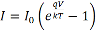
where:
I = the net current flowing through the diode;
I0 = "dark saturation current", the diode leakage current density in the absence of light;
V = applied voltage across the terminals of the diode;
q = absolute value of electron charge;
k = Boltzmann's constant; and
T = absolute temperature (K).
The "dark saturation current" (I0) is an extremely important parameter which differentiates one diode from another. I0 is a measure of the recombination in a device. A diode with a larger recombination will have a larger I0.
Note that:
I0 increases as T increases; and I0 decreases as material quality increases.
At 300K, kT/q = 25.85 mV, the "thermal voltage".
Non-Ideal Diodes
For actual diodes, the expression becomes:
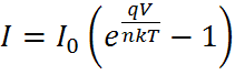
where:
n = ideality factor, a number between 1 and 2 which typically increases as the current decreases.
The diode law is illustrated for silicon.
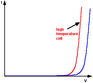
The diode law for silicon - current changes with voltage and temperature. For a given current, the curve shifts by approximately 2 mV/°C.
Acknowledgement


This web page is an adapted version of the article at the PVCDROM web site (with permission from the authors Stuart Bowden and Christiana Honsberg).
More about semiconductors
- Principles of Semiconductor Devices by Bart van Zeghbroeck, University of Colorado
- Semiconductor Tutorial by N. Cheung, U.C. Berkeley
- Semiconductors by Tony Kuphaldt,chapter III, on-line books series at allaboutcircuits.com
- Electrical Engineering Training Series from Integrated Publishing
- Britney Spears Guide To Semiconductor Physics