
From microelectronics to nanoelectronics
The evolution of electronics in the past forty years has been dominated by the idea of scaling the basic constituent of integrated circuits (ICs) - the metal-oxide-semiconductor (MOS) field-effect transistor (FET). Starting from the original device, with gate on the 10²-µm length scale, the MOSFET has evolved to the current one, with gate length of 45 nm at the production forefront. In so doing the complexity of CMOS (complementary MOS) ICs has evolved from the original small scale integration (SSI) to the current giga scale integration (GSI), where a single chip of area of the order of 1 cm² hosts several gigabits[1].
Transistors with much smaller gate length can be produced either via electron beam lithography or by subtractive techniques from lithographic features. These demonstrators have shown that the MOSFET can be scaled to the 10 nm length scale, preserving electrical characteristics still allowing its application for CMOS ICs.
Producing such small transistors, however, does not imply the existence of a 10-nm technology. Such a technology would indeed imply the possibility of defining and aligning all levels (active regions, sources and drains, contacts, metals, etc.) on a length scale of 10 nm. Denoting with F the minimum feature size (F = P/2, with P being the minimum pitch allowed by the considered lithography), the most dense memory architecture requires an area of 4F² per cell. At the F = 45-nm node this implies a local density of 1.2x1010 cm-2 that should increase to 5x1010 cm-2 at the F = 22-nm node.
Although continuing to climb the complexity scale seems technically possible (first to F = 16 nm and eventually to F = 11 nm), the increase of investment costs necessary for that is forecast to be an insurmountable wall for most players. While this barrier is an important strategic advantage for the largest players, it may be lethal for small players.
This state of affairs has fuelled the interest toward other architectures and technologies. Among the new architectures the crossbar one has had a key role because in principle it allows the preparation of matrices of cross-points, each embedding a material able to work by itself as a memory element [2]. In ultimate analysis the crossbar architecture is defined by two planar arrays of perpendicularly aligned conductive wires, separated by rectifying layer with two resistance states, RON and ROFF, with RON << ROFF, and so different to allow their external recognition.
In the crossbar structure the area per bit is given by 4F², so that the density allowed by this structure is the same as for the standard flash memory CMOS technology with NAND architecture. Therefore, the transition from the CMOS to the crossbar technology would not be sustained by any competitive advantage. In view of the conservative attitude of the industry, this situation would thus be unable to produce any technology shift were it not for the fact that the crossbar structure is producible with feature size f (or pitch p) well beneath the lithographic feature size F (or pitch P).
Managing sublithographic devices poses three major problems [1]: - their preparation; - their linkage to the external world through lithographically defined contacts; - the identification, preparation, and deposition of the functional material.
Sublithographic preparation of crossbar
In last years techniques not involving the use of advanced lithography have been developed for the preparation of nanometer-sized features; they are based on the transformation of vertical features into horizontal features and the most advanced ones allow the preparation of controlled lines with width of 10-20 nm. Although this strategy allows the preparation of simple geometries only (line arrays), the development of the crossbar architecture makes up for this inherent limitation; this structure is particularly attractive not only because it may simply be produced by crossing two perpendicularly oriented wire arrays but also because there exist different functional materials that can be used for the separation between upper and lower arrays.
Superlattice nanowire pattern transfer
The first method for the non-lithographic preparation of ultra-dense line arrays was originally proposed by Natelson et al. [3]. It is essentially based on the sequential alternate deposition of two films A and B characterized by the existence of a preferential etch for one of them (say, A). After cutting at 90° of a multilayer film ABAB...AB, polishing, and controlled etching of A, one eventually gets a mold that can be used as a mask for imprint lithography (IL). Actually IL is a contact (rather than proximity) lithography; what is non-lithographic is uniquely the way used for the preparation of the mask. The first practical application of this idea was provided by Melosh et al., who prepared a contact mask for IL with pitch of 16 nm by growing on a substrate a quantum well via molecular beam epitaxy, cutting the sample perpendicularly to the surface, polishing the newly exposed surface, and etching selectively the different strata of the well. If A and B are crystalline and their thickness does not vary from one deposition to another, the multilayer ABAB...AB is a superlattice-that has led to defining this trechnology as superlattice nanowire pattern transfer (SNAP) [4].
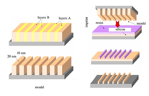
Figure: 1
Multi-sidewall patterning techniques
Another route for the non-lithographic preparation of ultra-dense line arrays is the multi-sidewall patterning technique (SnPT). This technology is able to produce wire arrays with pitch on the nanometer length scale exploiting an already existing IC technology-the sidewall patterning technique (SPT)-of conventional use in microelectronics for the self-alignment of the gate electrode on source-and-drain regions. In this way the SnPT may be viewed as a conservative extension of the current IC technology to the nanoscale length scale [1].
Multi-sidewall patterning techniques
I. Additive route
In the additive route of SnPT (referred to as SnPT+) an array of 2n wires is directly defined onto a substrate via a sequence of n conformal depositions and anisotropic etchings without etching the original seed used for the definition of the first sidewall. The basic idea underlying SnPT+ as originally proposed in [5],[6] is sketched in Figure 2. Although cross-point density of 8x1010 cm-2 could be achieved within the current technology, the overall process would however require 20 repetitions of each SPT cycle.
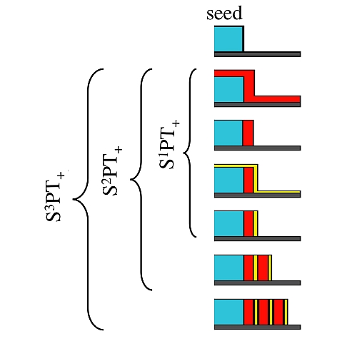
Figure: 2
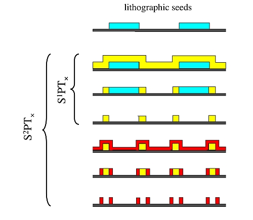
Figure: 3
II. Multiplicative route
Managing so many deposition-etching cycles may be difficult and expensive. Observing that the SPT allows, starting from one seed, the preparation of two bars, the above difficulty may be removed using a multiplicative variant (referred to as SnPTx) of the multi-sidewall patterning technique. SnPTx requires that each newly grown spacer is used as seed for the subsequent growth-that is possible if the original seed is etched away at the end of any cycle. In SnPTx each SnPTx cycle involves therefore the following steps: (1) the conformal deposition of a film on an assigned seed of high aspect ratio, (2) anisotropic etching of the film down to the appearance of the original seed, and (3) the selective etching of the seed.
Figure 3 sketches the basic idea underlying SPTx and shows that the material nature changes on going from one set of spacers to the subsequent one, so that the spacer material alternates, in our preferred embodiment, between poly-silicon and SiO2. Since the wire material is poly-silicon, the seed material depends on the parity of n: if is even, the seed should be in poly-silicon; otherwise in SiO2. The first demonstrators of SnPTx for the generation of gratings sub-lithographic pitch go back to more than a score of years [7]; the usefulness of this technique for the preparation of wire arrays potentially useful for biochips, instead, is much more recent [8],[9].
Linking the sublithographic crossbar to the external world
Even the definition of nano-object is subjected to discussion: the common definition (for which a device is a nanodevice when least one of its dimensions should be between 1 and 100 nm in size, and the tiny size of the device must be essential to its function) is unable to capture the common feeling in electronics for which "nano" means "not accessible via photololithography". In fact, although the availability of nanofabrication techniques is fundamental in establishing a nanotechnology, not less vital is the ntegration of the nanostructures with higher-level structures. The difficulties in communication between the nanoworld (not lithographically accessible) and the macroworld represent a central issue in the development of nanotechnology [10].
In view of its fundamental role in electronics, the problem can be limited to that of addressing the sublithpographic wires defining the crossbar by means of lithographic contacts. Several strategies have been adopted to attack this problem. Ignoring those based on a stochastic addressing (for which it is not known which cross-point is addressed and a complicate learning stage eliminating unaddressed cells and possibly exploiting redundancy [11]-[13]), nanoscopic wires can be addressed by means of the techniques employing horizontal bevelling (HBT), filled indentation (FIT), or energetic filtering (EFT). Contrarily to the methods based on stochastic addressing, all these methods are fully consistent with the existing silicon planar technology. However, whereas the HBT can be used irrespective of the crossbar preparation technique (SNAP, SnPTx, or SnPT+), the FCT and EFT can be used for SnPT+ crossbars only.
Horizontal bevelling technique
The HBT is reminiscent of the bevelling technique once used, together with microsectioning and staining, for the measurement of junction depth (and more recently of carrier concentration profiles via measurement of spreading resistance).
To contact separately each wire in a sublithographic array, after the deposition of a protective insulating cap a thin trench (of width around f) is cut, tilted by an angle α with respect to the array and so long as to cross all wires. This process results in the exposition of 2n rhomboids with pitch p in the direction perpendicular to the array and p/tan(α) in the direction of the array. It is thus sufficient to take α > artan(p/P) to allow the separate lithographic contact to the wires. Figure 4 sketches the resulting pattern.
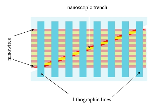
Figure: 4
Filled indentation technique
The FCT requires that the mask used as a seed for the SnPT+ has a pattern deviating from the rectilinear one by 2n indentiations of widths wk, wk= w0 + (k-1) w1, with w1 = 2p and k = 1,..., 2n. What is interesting in this pattern is that if 2p<w0<2.5p, any metallic shunt of width F<w0 centered of the central region of the k-th indentation contacts exclusively the k-th wire [14]. The minimum sublithographic feature size fmin that can be lithographically contacted with the FCT is therefore given by fmin = 0.2F (that would give fmin = 9 nm at the F=45-nm node).
Energetic filtering technique
Whereas in SNAP and SnPTx all wires are defined collectively, in SnPT+ they are constructed sequentially. The batch fabrication would make SNAP and SnPTx preferable over SnPT+ unless one were able to use the sequential array deposition for the external recognition of single wires.
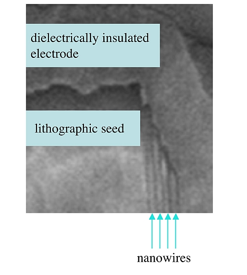
Figure: 5
An inspection of the right side of Figure 5 shows that SnPT+ results in wires whose height is progressively reduced with the order of preparation. This spatial difference for the recognition and separation of single nanoscopic wires by electrical probes simply by controlling capacitively the conduction state of each wire.
This structure allows in principle a dramatic simplification in the contact architecture: while the HBT and FIT require 2n contacts to address n2 cross-points, the EFT requires 2+2 dielectrically insulated electrodes and 2 ohmic contacts. This simplicity is however paid in terms of the decoding circuitry required to extract from the measured current the actual state of each cross-point [15].
Choice, preparation, and deposition of the functional material
Together with its producibility on a sublithographic length scale, the crossbar has another great advantage:it allows the preparation of non volatile memories simply by separating upper and lower arrays with a resistive material displaying suitable hysteresis properties. This would be a mere declaration of principle were it not for the fact that materials with this property already exist-for instance, phase change materials. There is however a strong interest for other materials (exploiting, for instance, ionic conduction [16]). Among the candidate materials, since the discovery of rectifying properties of molecules [17] and the report of a molecule displaying resonant conduction [18], electrically programmable molecules play a special role. Although demonstrators based on rotaxanes have been presented [19], their integration with silicon for the preparation of hybrid devices has been shown to be difficult. A strategy for that has been described in Ref. [20].
Acknowledgement

Materials at the web page were presented by Professor Gianfranco Cerofolini, Department of Materials Science, University of Milano Bicocca, Italy.
References
[1] For a general overview of this topic see G. F. Cerofolini, Nanoscale Devices (Springer-Verlag, Berlin, 2009).
[2] Heath J. R., Kuekes P. J., Snider G. S., Williams R. S., "A defect-tolerant computer architecture: Opportunities for nanotechnology", Science 280, 1716 (1998).
[3] Natelson D., Willett R. L., West K. W., Pfeiffer L. N., "Fabrication of extremely narrow metal wires", Appl. Phys. Lett. 77, 1991 (2000).
[4] Heath J. R., "Superlattice nanowire pattern transfer (SNAP)", Acc. Chem. Res. 41, 1609 (2008).
[5] Cerofolini G. F., Arena G., Camalleri M., Galati C., Reina S., Renna L., Mascolo D., Nosik V., "Strategies for nanoelectronics", Microelectr. Eng. 81, 405 (2005).
[6] Flanders D. C., Efremow N. N., "Generation of < 50 nm period gratings using edge defined techniques", J. Vac. Sci. Technol. B 1, 1105 (1983).
[7] Flanders D. C., Efremow N. N., "Generation of < 50 nm period gratings using edge defined techniques", J. Vac. Sci. Technol. B 1, 1105 (1983).
[8] Choi Y.-K., Zhu J., Grunes J., Bokor J., Somorjai G.A., "Fabrication of sub-10-nm silicon nanowire arrays by size reduction lithography", J. Phys. Chem. B 107, 3340 (2003).
[9] Choi Y.-K., Lee J. S., Zhu J., Somorjai G. A., Lee L. P., Bokor J., "Sublithographic nanofabrication technology for nanocatalysts and DNA chips", J. Vac. Sci. Technol. B 21, 2951 (2003).
[10] Roukes M., "Plenty of room indeed", Sci. Am. Repts. 17 (No. 3) 4 (2007).
[11] Huang Y., Duan X., Cui Y., Lauhon L. J., Kim K.-H., Lieber C. M., "Logic gates and computation from assembled nanowire building blocks", Science 294, 1313 (2001).
[12] Zhong Z., Wang D., Cui Y., Bockrath M. W., Lieber C. M., "Nanowire crossbar arrays as address decoders for integrated nanosystems", Science 302, 1377 (2003).
[13] Strukov D. B., Likharev K. K., "Prospects for terabit-scale nanoelectronic memories", Nanotechnology 16, 137 (2005).
[14] Cerofolini G. F., Mascolo D., "A hybrid route from CMOS to nano and molecular electronics", in Nanotechnology for Electronic Materials and Devices, edited by Gusev E., Korkin A., Labanowski J., Luryi S. (Springer, New York, 2006) pp. 1.
[15] Cerofolini G. F., "Realistic limits to computation. II. The technological side", Appl. Phys. A 86, 31 (2007).
[16] Despotuli A. L., Andreeva A.V., Rambabu B.,"Nanoionics of advanced superionic conductors", Ionics 11, 306 (2005).
[17] Aviram A., Ratner M.A., "Molecular rectifiers", Chem. Phys. Lett. 29, 277 (1974).
[18] Chen J., Reed M. A., Rawlett A. M., Tour J. M., "Large on-off ratios and negative differential resistance in a molecular electronic device", Science 286, 1550 (1999).
[19] Luo Y., Collier C. P., Jeppesen J. O., Nielsen K. A., Delonno E., Ho G., Perkins J., Tseng H.-R., Yamamoto T., Stoddart J. F., Heath J. R., "Two-dimensional molecular electronics circuits", Chem. Phys. Chem. 3, 519 (2002).
[20] Cerofolini G. F., Romano E., "Molecular electronics in silicon", Appl. Phys. A 91, 181 (2008).