
Thin Film Deposition

Do You Want to Know About Thin Film?
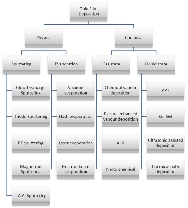
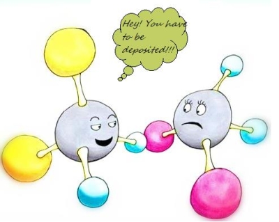
Thin film deposition is one of the most required techniques in vacuum technology that is required for a variety of application in mainly material science."Thin" is a relative term.
It's very interesting to know how we can make and process a thin film. As you know most deposition techniques control layer thickness within a few tens of nanometers. Also Thin film can be produced by certain way. Let's discuss! Well there is some process name as drop casting and then oil bathing subsequently, can be produced through spin coating, by plasma sputtering, by chemical deposition etc. Mother Nature gives us a lot of things using which we can produce a lot of things! Okay, let's discuss about some process. Spin coating or spin casting, uses a liquid precursor, or sol-gel precursor deposited onto a flat substrate which is subsequently spun at a high velocity to centrifugally spread the solution over the substrate with a certain r.p.m. The spinning speed at which it is spun and the viscosity of the desired sol determines the thickness of the film. Isn't it funny! Yes it's really funny. Well let us continue.
How to Make Thin Film
So, now it’s time to tell how we can make a thin film. There are certain procedures to make thin film. We can do is physically, can make chemically also! Okay, here we focus on Physical Procedure named as physical vapour deposition. After that we will tell about Chemical vapour deposition (CVD), and then we will go for some other important deposition techniques.
PHYSICAL VAPOR DEPOSITION (PVD): This procedure covers a number of deposition technologies in which material is released from a source material and transferred to a substrate.
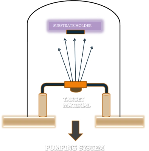
One of the common methods of Physical Vapor Deposition is Thermal Evaporation. This is actually a form of Thin Film Deposition. It is a technology using vacuum formalism for applying coatings of pure materials onto the surface of various substrates. The coatings, which are called films, are usually in the thickness range of angstroms to microns, in general. Here the object what is to be coated is referred to as the substrate, and can be any of a variety of things like quartz, glass plate, silicon etc. Thermal Evaporation is done by heating a solid material inside a high vacuum bell jar like chamber. Inside the vacuum, even a relatively low vapor pressure is very sufficient to produce a vapor cloud inside the deposition chamber. The evaporated material now constitutes a vapor stream which traverses into the vacant chamber and hits the surface of the substrate, sticking to it as a coating or film. Since, in most instances of thermal evaporation processes the material, is heated naturally to its melting point, it is usually located in the bottom of the chamber with a screw along with the holder. The vapor then rises above from this bottom source, and the substrates are held inverted in appropriate fixtures at the top of the chamber so that the deposition can be occurs in the desired area of the substrate. The surfaces of the substrate, which are to be coated are facing down towards the heated source material (like Al, Ag etc. many more) to receive their desired coating.
The main procedure of heating the source material is Filament Evaporation, is a simple electrical resistive heat element of filament. One may take Tungsten filament (The filament source offers the safety of low voltage, although very high current is required, usually several hundred amps).Here the evaporation rate is determined by the vapor pressure of the source material and the evaporation temperature. Let’s we take that elements for evaporation whose melting point is less than 1400 degree Celsius (Think we pass 0.400A current through Tungsten filament); Here one may take various metals like Al, Ag etc. for evaporating material. A deposition chamber under high vacuum (~10-6 m.bar) is necessary in order to avoid the oxidation of source material.
We can use two Gauges here named Pirani Gauge and Penning Gauge which are used for measuring the pressure in vacuum system. Penning gauge is usually used for measuring the pressure below 10-3 Torr and it is very sensitive due to random pressure fluctuation.
CHEMICAL VAPOR DEPOSITION: Let’s go towards what CVD actually is. Like PVD it is also a deposition technique. In CVD process, thin film of several materials can be deposited onto the faces of a substrate with some chemical reactions of gas molecules which contain the needed atoms for the growth of the thin film. In this case the materials are used as volatile molecules which we can call as precursors, and these precursors and the substrate contribute jointly for the growth of thin film via some chemical reactions between them. Diffusion process takes an important role for the deposition.
But during these process some by-products are also produced which can be removed by a gas flow inside the chamber of reaction. For producing high quality thin film, CVD is often used in the industry of semi conductors. The carrier gas in CVD is mostly the mixtures of hydrogen, argon, nitrogen and also their compositions. There are several types of CVD, Let’s try to introduce them!
- High Temperature CVD: For the deposition of Silicon or some compound coatings like Titanium Nitride, high temperature is needed to activate CVD process thermally in the temperature range of 200-1500 degree Celsius.
- Low Temperature CVD: If we want to deposit some insulating layers as a thin film like silicon dioxide, very low temperature has to be gained for better depositions.
- Low Pressure CVD: Some of the deposition like silicon carbide needs lower pressure for higher performances.
- Plasma Assisted CVD: There are some depositon processes that use plasma to activate the ractions by generating ions as well as electron collisions are known as Plasma assisted CVD or Plasma Enhanced CVD.
- Photo Assisted CVD: The photons emerged from a laser can also activate the chemistry of the vapour phase regarding the CVD.
WHY WE USE CVD?
Now guys it’s time to tell why we use CVD so widely in our daily life..So, Let’s discuss with that also! Well, there are a lot of impacts of CVD in our society. Functional coating of transparent SnO2 :F are used widely for coating the window glasses for the need of cooling down or warming up of our rooms..Again for the darkness of the glasses via thermochromism process thin films of VO2 is used we all know. Again we use sunlight for photocatalysis process to break the dirt and hence make self-cleaning glasses. The whole Microelectronics industry stands upon this CVD process to hold their highly controlled electrical properties also. For teli communication we all know that Optical fibre is used. Even to produce optoelectronic devices, sensors, CVD is a highly useful process.

PVD VS CVD: WHEN TO USE WHAT!!!
Well, we learn two methods for deposition of thin film. A natural question should come in our mind that when we use what method for thin film deposition! Okay! Let’s discuss over that! To be frank, depending on application and situation we have to choose either process. We saw that we need specialized precursor materials for CVD but sputtering process in PVD doesn’t need any precursors as well.
The Temperature dependence is one of the most important distinctions between these two processes. We saw that CVD needs higher temperature than PVD, which plays important role in between 400 – 1000 degree Celsius for CVD, there are some material whose boiling point doesn’t permit to use CVD for the growth of thin film as those materials are playing as substrates. So in that case PVD has to be played. Again for some cases CVD is done as this process takes less waste deposition.
Though PVD and CVD are the two main method for the growth of a thin film, still there is some another methods regarding this deposition. Some of are discussed below-
SOL-GEL METHOD: Okay!! Let’s discuss about another interesting one! Its called Sol-Gel technique for synthesizing transition metal oxides. For synthesizing oxide materials Sol-Gel technique is widely used in thin film industries. If you want to deposit many component materials then by this method homogeneity is purely maintained mostly. Here SOL stands for the formation of solution of composite materials as colloids and GEL is the viscous formation of that SOL. This method is useful under lower temperature indeed. Though there are some methods of sol-gel preparation, but basically they works in a similar way in which a vast quantity of nano scale materials are produced for deposition with it’s well controlled orientation as well as particle size. Let’s discuss the process schematically.
ATOMIC LAYER DEPOSITION: If you want a smaller as well as a ultra miniature version of thin film where standard of performance is still has to be maintained properly, then probably ALD is one of the best method you can use! This process can be thought as a sub section of CVD also. Deposition can be growth via this method by some sequences of vapour phase chemical procedure. In this method precursors are exhausted in a periodic manner like as a pulse in non overlapping way inside the region where reaction is occurred. By varying the number of such cycle we can deposit uniform monolayer of thin film onto the substrate. As the electronic materials become smaller by using this method, there is a huge application based popularity of this ALD in semiconductor industries. To produce nanomaterials, there is a large contribution of this technique. In biomedical industry, there is a large application of ALD in tissue engineering also! It’s really awesome to know the exposure of Thin Film Technology, Isn’t it?
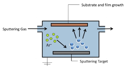
PLASMA SPUTTERING: Now it’s time to introduce plasma ejection! Here atoms are sputtered by colliding energized atoms like Ar+ with the solid target materials. Hence ejected atoms are deposited onto the substrate as thin film. In some case partly ionized plasma system which contains free electrons are required to ionize the atoms of neutral gas at high vacuum. Here Re-sputtering process also has to be done for discharging of deposited material via atomic bombardment. Here momentum transfer between the atoms plays the main role inside the sputtering vacuum chamber.
WHY ARE WE MAKING THIN FILM!
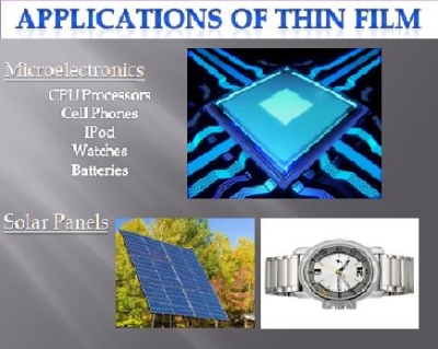
Oh! it's time to tell about why we are going to make Thin Film...Certainly there is some Usage.Our society overlooks the importance of vacuum coatings in products they use. The semiconductor industry relies broadly on thin film technology to produce flash memory and computer chips and a lot of things also. A lot of industries produce optical products and use polarizer (optical) and beam splitters in their designs to form their products. Other industries also use thin film technology most of which is for cosmetic purposes, like mirrors apart from these toys are also made using Thin Film! It is useful in the manufacture of optics (for reflective as well as anti-reflective coatings, self-cleaning glass), optoelectronics (for manufacturing of ICs, LED, OLED devices, LCDs, CMOS, camera sensors), electronics (layers of various insulators, semiconductor thin film, and conductors form integrated circuits). Thin-film technology is also being developed now-a-days for reducing the cost of solar cells. The fundamental for this thin-film solar cells are cheaper to manufacture because of their reduced material costs, handling costs, production cost. It plays a big role in solar collector coating for increasing the efficiency of photo-thermal conversion, photovoltaic cells also. In Nanotechnology, it helps to improve size effects by coating of nano materials via magnetron sputtering. Our daily useful wrist watches, knives are coated by deposition procedure to protect from corrosion also! So it is proved that Thin Film contributes a lot of field in our daily life activity and become an essential aspect of our lifestyle.
I think this helps you a lot to know about the thin film. I hope you all shall start to study in detailed manner about these special tools in further. Thank you. Best of luck!
Acknowledgement

Content of the web page has been developed by Souvik Kumar Naskar, MSc. Physics student of Indian Institute Of Technology Guwahati.