
Nanotechnology Today
 There are many reasonable definitions of technology in general, and nanotechnology - in particular. Depending on definition, our perception of nanotechnology may be as a dream about relatively remote future, or actual state of the nowadays hi-tech.
1st Definition: Technology becomes “nano” when it produces new kind of artifacts due to a nanometer-range resolution at least in one of three dimensions. In this definition, ‘nano’ firstly started in the time of WWII with thin optical coatings, and finally - in the middle of 1950s with introduction of ‘double-diffused’ transistor.
2nd Definition: Technology becomes “nano” when it produces new kind of artifacts due to a nanometer-range resolution in all three dimensions. In this definition, ‘nano’ was born at the border 1980s-1990s, when the design rule in semiconductor industry was firmly established below 1μm ‘waterline’. It had matured at early 2000s while submerging bellow 100 nm.
3rd Definition: Technology becomes “nano” producing intelligent products without direct external intervention (by self-organization). In this definition, we now almost exactly in the middle of the road to Nanotechnology from its conception at 1950s.
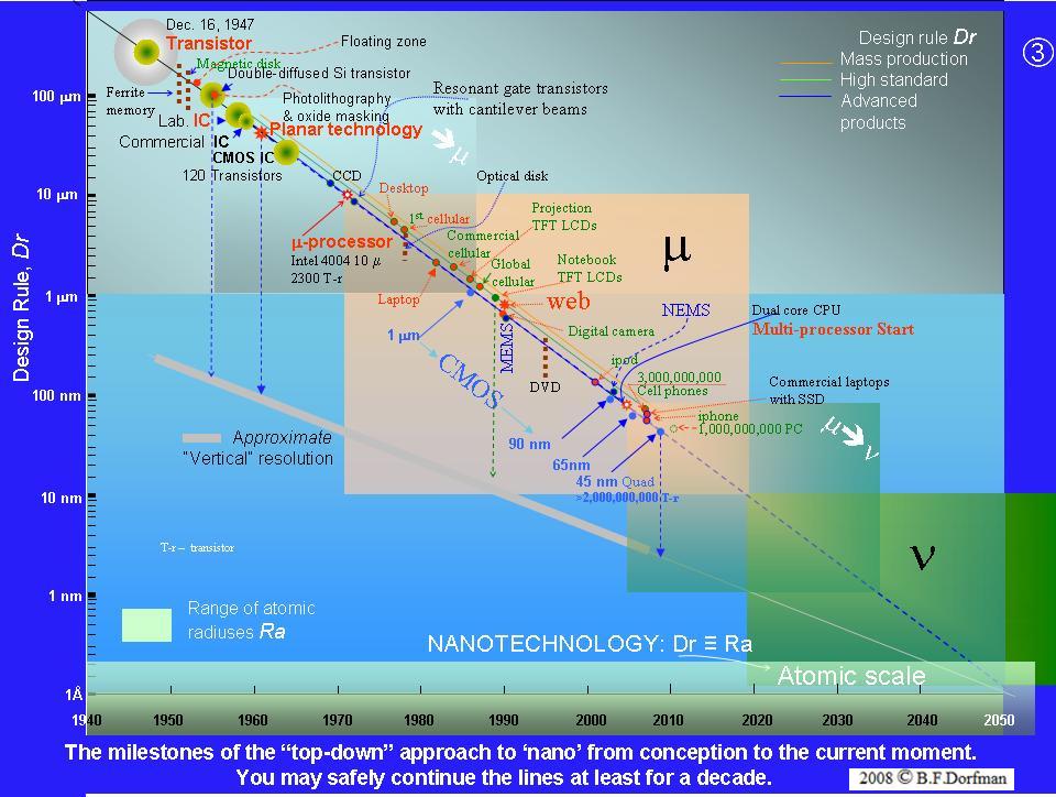
‘Football field’ on Intel’ chip: up to ˜ 2,000,000,000 transistors/ 45 nanometer ‘design rule’. To make 45 nm visible, we must magnify ˜ 1 cm chip to a real football field (the heads of players may be hit by satellites). This - a current cutting edge of “top-down” approach: steady progress of hi-tech’ resolution to atomic scale.
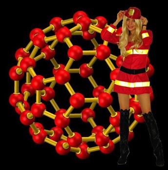
 Two players fight for 540-atom buckyball - a cutting edge in some direction of progress in the “bottom-up” approach: from atomic scale to products. Even at such magnification, buckyball is almost unnoticeable; it will need two more orders of magnification to distinguish its details.
True nanotechnology will only start at the point where the “design rules” of “top-down” and “bottom-top” approaches will be equalized & synergized - ˜ 3-4 decades from now. But so far, altering the world ˜800,000,000 PCs, > 3,000,000,000 cell phones, Internet, library on disk, ipod, digital cameras, medical sensors, flat TV, more accurate weather prognosis, computer-assisted design of the technology itself, - are based on ‘top-down’ nano-progress.
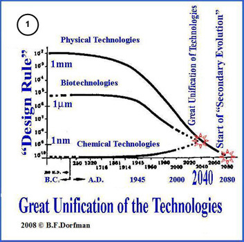
Nanotechnology is not a specific technology, or specific technologies, it is the Great Unification of the Technologies in a relatively near future (˜2040). Figures 1 and 2 are from the book: ‘Evolutions of technologies, or New history of the Time’ (B.F. Dorfman, Moscow, 1990, in Russian).
 Progress 1cm→1mm - ˜10,000 years, 1mm→100mm - century, 100μm→100nm ˜½ century + another ½ century to reach atomic scale.
On diagram 1, the historical time scale is not linear because the real time of progress was not linear. New universe was in a latent state up to the Middle-Age mechanics (clocks and automats), it became visible with the first Industrial Revolution, exploded with the Second one. But the real ‘Big bang’ was transistor. From that moment and over half a century it is almost strictly linear: diagram 3 on the following screen.
Nanotechnology ≡ Great Unification of the Technologies
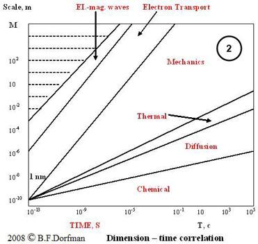
Approaching the atomic-scale in geometric dimensions, most of physical phenomena are nearly equalizing in the time (→speed) dimension. This may change our ‘common sense’. For instance, electromechanical relays, which were once starting points for both theory and practically working computers, - may return as the best known digital element, but on molecular base. (To make a relay-equivalent for PC-2010, one would need some megaton of relays, gigaton of wire, gigawatt of power, millennium for realization and astronomical time for system operation).
Electronics: From Micro to Nano
Transistor was a truly revolutionary invention for human communication, and a key device for logics and memory elements of modern electronics. The practical and essentially reciprocal history of unipolar and bipolar transistors started after the Second World War. The junction transistor was invented by William Shockley and later Brattain and Bardeen have created the first [germanium] bipolar transistor. Bardeen provided theoretical explanation why the original Shockley’s FET did not work (imperfect surface "killing" the free carriers of electrical charge), while Shockely developed the fundamental theory of Electrons and Holes in Semiconductors (1950) first employed for bipolar transistors. As soon as the concept of the planar transistor was established, Robert Noyce suggested formation of interconnects on the same silicon substrate.
Independently, the idea to form wires connecting undivided transistors on substrate was suggested in Texas Instruments by Jack Kilby. To the middle of 1960s, the planar technology of silicon integrated circuits, including surface treatment, had matured resulting to more compact and less energy consuming devices especially in complimentary pairs of CMOS (p-channel & n-channel transistors). In the last decades the progress of electronics industry has been primarily based on scaling down transistors and other electronics devices to smaller and smaller devices approaching the fundamental limits of materials capacity to function according to the requirements of information processing and storage without breaking up (short cut and diffusion). The GIGA challenges at NANO scale open the doors for new paradigms in information technology.
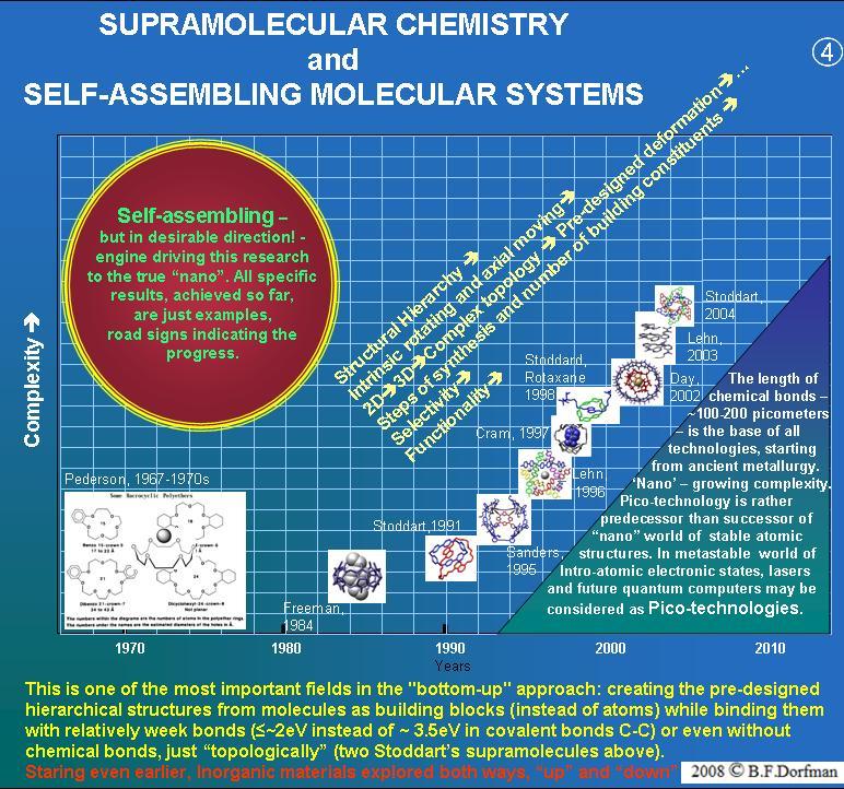
Supramolecular Chemistry: From Pico to Nano
In the first ‘crown ethers’ - ancestors of the entire field (shown in the left bottom corner of the diagram), the size of their most remarkable feature - cavity - is in the range of 120 to 320 pico-meters. Hierarchical supramolecules synthesized in 2000s preserve such pico-feature while adding also next floors, e.g. ‘nano’ levels. Differently from semiconductor’s “nano”, where the world’ leader Intel alone has ˜90,000 employees, supramolecular chemistry is still more academic field, and every step of progress associated with individual name of discoverer.
Acknowledgement

This web page is an adapted version of the article published at Secondbang Blogpost by Benjamin Dorfman (with permission from the author). Photos by Natalie and Dwight Hanson
Some links suggested for further reading:
- A Saga of Semiconductor Technology Transfer by Michael Riordan
- From the Lab to the Fab: Transistors to Intergarted Circuits by Howard Huff
- IBM Shines Light on 22 nm Chip Manufacturing
- ISMI Outlines 450 mm Wafer
- The Discovery of Crown Ethers by Charles Pedersen
- Supramolecular Chemistry by Jean-Marie Lehn
- Supramolecular Chemistry: Functional Structures on the Meso Scale
- Nanotechnology Encyclopedia: Supramolecular Chemistry
YouTube Videos
Nanotechnology Takes Off
Age of Convergence
Journey Into Nanotechnology
How Nanotechnology Works