
Atomic Scale Memory at a Silicon Surface
Do atoms have memory? If they did, it would be possible for anybody to store a full collection of music, videos, and movies on a memory stick, plus all the books in the Library of Congress, with room to spare. And the answer to this question is YES: Nanotechnology makes it possible to use a single atom to store a bit, the fundamental unit of information (YES or NO). Atoms can be positioned precisely at the surface of a silicon chip. One can tell whether or not an atom is at its assigned position (its home address). If it is home, that means a YES, if it is not, that means a NO. In the following, a prototype memory of this type will be described. In case you want to buy such a memory stick, you still have to wait a bit: According to Moore´s law of silicon technology we will not reach such a high density of bits commercially until the year 2038 – assuming Moore´s law holds that long.
In his landmark 1959 talk at Caltech, Richard Feynman estimated that ‘all of the information that man has carefully accumulated in all the books in the world, can be written … in a cube of material one two-hundredth of an inch wide’. Thereby, he uses a cube of 5 x 5 x 5 = 125 atoms to store one bit, which is comparable to the 32 atoms that store one bit in DNA. Such a simple, back-of-the-envelope calculation gave a first glimpse into how much room there is for improving the density of stored data when going down to the atomic level. In the meantime, there has been great progress towards miniaturizing electronic devices. Our pocket size computers and no less sophisticated cell phones have the same or even higher speed and memory than monstrous computers in 1960s, which occupied a few large rooms!
One important consideration for memory devices is how closely can the bits be packed without interacting, which means that reading, writing or storage of the information is not influenced by neighboring elementary memory devices. Using our household analogy we are talking about a situation of an inspector nocking on the door of the house, while his tenant went to a party (interaction) with his neighbor. In this case “reading” would provide a wrong (zero) answer regarding the home occupancy. In case of the atoms the most foreseeable situation leading to loss of memory would be thermal diffusion which allows one atom to jump to a vacant spot. This would result to loss of the right information at both bits!
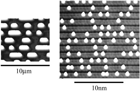
A two-dimensional version of Feynman's atomic memory can be formed on the surface of silicon by a small amount of gold (below on the right). It looks similar to the CD-ROM on the left, but the scale is in nanometers instead of micrometers. Thefore, the storage density is a million times higher. The gold triggers the formation of self-assembled tracks, which are exactly five atoms wide. Extra silicon atoms sit on top of the tracks in well-defined positions. It is suggestive to assign an extra silicon atom to a 1 and a vacancy to a 0. The minimum empty area required around each bit is 5 x 4 = 20 atoms, 4 atoms along the track and 5 atoms from one track to the next. Feynman's 1959 suggestion of spacing the bits 5 atoms apart was right on the mark.
Reading and writing
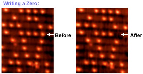
Reading the memory consists of a simple, line scan with a scanning tunneling microscope (STM) along the self-assembled tracks. There is no need to search in two dimensions for the location of a bit. The signal is highly predictable since all atoms have the same shape and sit on well-defined lattice sites. That allows for a high level of filtering and error correction. Writing is more difficult. While loosely-attached surface atoms can be moved around with a STM at liquid helium temperature, that is much harder to achieve that at room temperature. In order to prevent them from moving around spontaneously, it is necessary to choose atoms that are strongly bound to the surface. Pushing them around with the STM tip requires a close approach and often leads to atoms jumping over to the tip. This problem can be turned into a solution by using the STM tip to remove a silicon atom for writing a 0. The memory is pre-formatted with 1 everywhere by depositing silicon atoms onto all vacant sites.
Reliability and speed
Reliability and speed are key issues with atomic scale memory cells. Correlations between adjacent bits come into play at high storage density. In magnetic storage one has to be concerned about magnetic coupling between adjacent particles at a bit spacing of 10 nm or less. By investigating a storage device at the single atom limit one can learn something about how today's data storage might evolve in the future. The graph below shows readout speed versus storage density, two key properties of a memory. Compared to traditional data storage in hard disks, the silicon atom memory has a very impressive density (250 Terabits per square inch), but its data rate is extremely low.
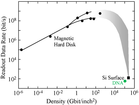
As the size of a bit shrinks, less energy that can be extracted from it during readout. Therefore, one needs a longer integration time for obtaining an acceptable signal-to-noise level. Even the theoretical limit of the data rate with the best possible readout electronics (top of the shaded region) is still lower than what hard disks achieve today. In the future, we can expect a tradeoff between density and speed. Actually, the data rate of hard disks shows signs of leveling out already. The data rate will have to be recovered by a high degree of parallelism, such as many reading heads and multiple disks.
Acknowledgement

This web page is an adapted version of the article "Atomic scale memory at a silicon surface" by Franz Himpsel published in Nanotechnology, v. 13 (4), 2002, pp. 499-502 (with permission from the author and the IOP Publishing).
More from and about Franz Himpsel
- BBC News about Atomic Scale Memory
- Davisson-Germer Prize
- Microscopic structure of the SiO2/Si interface
- Magnetic Nanostructures
- Quantum well states as mediators of magnetic coupling in superlattices