
Light Emitting Diodes (LEDs): A Look Inside
 LEDs have been around for about 30 years. They have found application everywhere, from glowing keychains to TV sets. Generally, an inorganic LED is a device comprised of a semiconductor with two differently doped regions: n-type (electron conducting) and p-type (hole conducting). Let's take a thorough look at them.
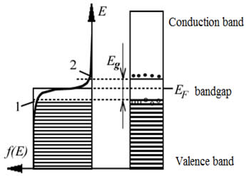
It is well known that a semiconductor becomes more electrically conductive through the absorption of electromagnetic radiation, e.g. visible light, ultraviolet, infrared, or gamma radiation. If the light absorbed by a semiconductor has energy higher than the band gap (Eg) electrons are able to jump from the valence to the conduction band and contribute to electrical conductivity of the semiconductor. Meanwhile the "empty spot" left by the electron in the valence band (the "hole") can be occupied by another electron in the valance band, which then becomes a source of hole conductivity.
While in the case of a single type of semiconductor we can observe an increase in conductivity when an external voltage is applied, two semiconductors of different type connected together (forming a "p-n-junction") can generate an electric field and electric current under the influence of incident radiation. This current arises due to electron-hole recombination. The current strength, in turn, depends on the intensity of the light absorbed by the semiconductor. If the light is turned off the current goes down.
How a LED Works
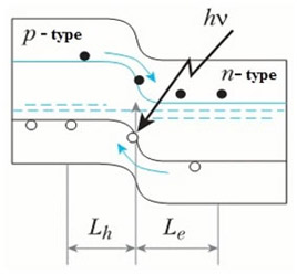
If a p-type semiconductor is connected to an anode and an n-type connected to a cathode, an interdiffusion of electrons and holes will occur in the region adjacent to the p-n-junction, driven by their concentration gradients. When an electron recombines with a hole, energy releases due to the transfer of the electron to a lower energy level. However, in a wide range of semiconductors, such as silicon or germanium, recombination of electrons and holes is not accompanied by emission of light but instead leads to an increase in the energy of vibrations (non-radiative transitions). Semiconductors of this type are called indirect band gap semiconductors. In order to make an LED, we need to make a p-n-junction with semiconductors having a direct band gap with energy corresponding to the energy of visible light photons. It is simple to distinguish these two types of semiconductors by their light transparency: semiconductors capable of releasing excess energy in the form of radiation are usually transparent to visible light. For instance, GaAs (gallium arsenide) and GaN (gallium nitride) are transparent semiconductors and they are well suited for manufacture of LEDs.
 If (forward) bias is applied, the number of charge carriers which are able to overcome the barrier and move across the p-n-junction will increase (this is "minority charge injection"). Simultaneously, the number of the majority carriers coming through the contacts increases as well, leading to charge compensation. As a result the rate of recombination goes up, and the resulting electric current grows exponentially as a function of the bias magnitude.
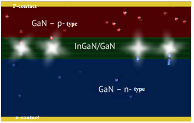
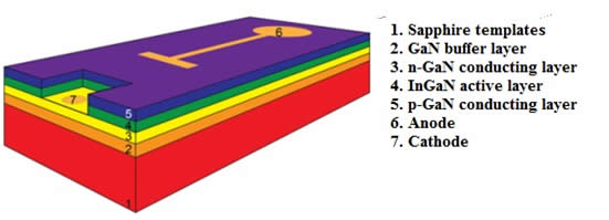
As previously mentioned, the recombination of electrons and holes in direct-gap semiconductors is accompanied by the emission of photons; the wavelength of emitted light depends on the band-gap energy of the semiconductor, which varies for different materials. For instance, gallium nitride, which is widely used in modern LEDs, is characterized by luminescence at a wavelength of 365 nm. One of the main problems in the manufacture of LEDs is to obtain defect-free GaN crystals, which are produced by epitaxial growth on sapphire templates. Modern commercial LEDs consisting of very thin (10-15 nm) alternating layers of p- and n-semiconductors are manufactured using MOCVD (metal-oxide chemical vapor deposition or chemical vapor deposition).
What are the advantages and disadvantages of LEDs?
Let's start with the disadvantages, which are very few. First of all, the light beam of an LED is usually less intense then the one from common light bulbs. Second, LEDs are typically characterized by a low color rendering index (CRI), which is a measure of the ability of a light source to reproduce the colors of various objects. Halogen lamps, for example, have a quite high CRI (> 90%), whereas conventional LEDs have CRIs in the range of 60-69%. It should be noted, however, that both of these problems are being solved successfully by manufacturers of modern LEDs.
 The benefits of LEDS cannot be overestimated. Modern LEDs can operate up to 50,000 hours and are characterized by significantly lower power consumption then conventional light sources. Moreover there are no harmful UV wavelengths in their radiation and it is possible to use them for production of "safe" tanning solariums. One of prospective applications of LEDs is in so-called "intelligent light systems", which combine super-efficient LEDs with sensors to provide "smart" (energy efficient) lighting. One of the main directions of LED technology development is the replacement of inorganic by organic materials. The operating principle of an organic LED (OLED) is based on the same physics as inorganic ones, but its design is quite different.
For efficient and long lasting operation, OLEDs require additional electron and hole conductive layers and hole-blocking layers. OLEDs have several advantages over LEDs. For example, they allow increasing the viewing angle, brightness, contrast, resolution, and size of the screens. Flexible screens which can be rolled into tubes can be manufactured using OLEDs. In the future, OLEDs will make it possible to manufacture luminescent wallpaper with images that can be changed, e.g. by downloading from the internet or by creating them from home-made photos or by using Photoshop. Imagine what you could do with entire walls in your house or apartment!
Acknowledgement
This article has been created by Ekaterina Polyutina as a short adapted version of the original articles, Simply about LEDs by Valentina Utochnikova and Look inside: LED bulbs by Eugine Smirnov, published at the Russian nanotechnology web portal Nanometer.ru. Translation by Taya Skorina.