
Electron Transport in Semiconductors
The subject of electronic transport in semiconductors and in solids in general, is a very old problem, which has been well studied over the past 75 years. Transport is an inherently non-equilibrium phenomena, where the role of dissipation and the coupling to the environment play a crucial role. External forces which drive the system out of equilibrium may be electromagnetic in origin, such as the electric fields associated with an applied DC bias, or the excitations of electrons from their ground to excited states due to high frequency optical excitation. Alternately, electrochemical potentials and thermal gradients may also provide the drive for electronic transport and its external manifestation in terms of macroscopic currents and voltages.
Electronic transport at its most fundamental level requires a full many body quantum mechanical description. Clearly, a full many particle description of transport including the real number of particles in both the device, its contact to the external environment, and the external environment itself, is beyond the ability of any computational platform in the foreseeable future. Hence, successive levels of approximation, that sacrifice information about the system, and the exact nature of transport, are necessary in any sort of realistic description of transport. the figure below illustrates the hierarchy of transport approaches used in describing electronic transport in semiconductors, metals, and molecular systems. At the bottom is the exact solution of the N-body quantum mechanical problem which is computationally intractable except for small numbers of particles (less than 100).
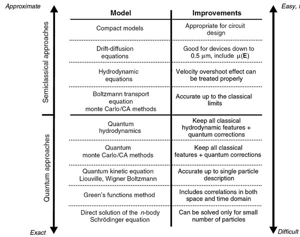
To treat the many-body problem, some sort of mean-field approximation is necessary which transforms the problem into an effective one-electron problem. Non-equilibrium Green function methods are currently popular at the next level of approximation as they contain retain important correlations in space and time, which are believed to be important at the nanoscale. Above this are quantum kinetic approaches in terms of the Liouville-von Neumann equation of motion for the density matrix, or Wigner distribution approaches that contain quantum correlations but retain the form of semi-classical approaches in terms of the distribution function. In going from the quantum to the classical description of charge transport, information concerning the phase of the electron and its non-local behavior are lost, and electronic transport is treated in terms of a purely particle framework.
This is the level of the Bolzmann transport equation (BTE), which represents a kinetic equation describing the time evolution of the distribution functionof the position and momentum of the particle, and has been the primary framework for describing transport in semiconductors and semiconductor devices with micro-scale and above dimensions. There are then approximations to the BTE, given by moment expansions of the BTE which lead to the hydrodynamic, the drift-diffusion, and relaxation time approximation approaches to transport. Finally, at an empirical level are non-linear circuit models for device behavior suitable for circuit simulation in so called compact models.
One interesting aspect of transport in nanostructure systems, is that the characteristic length scales span the transition from classical to quantum transport. Hence a single description in the hierarchy may not be sufficient, or may be overly cumbersome for providing the correct physics of device operation. Depending on certain critical length scales, transport may be semi-classical or purely quantum, or even more difficult, a mixture of the two in which the effects of decoherence and dissipation play important roles, while at the same time, quantum effects still dominant. To illustrate this notion, let us consider a prototypical nanodevice illustrated below:
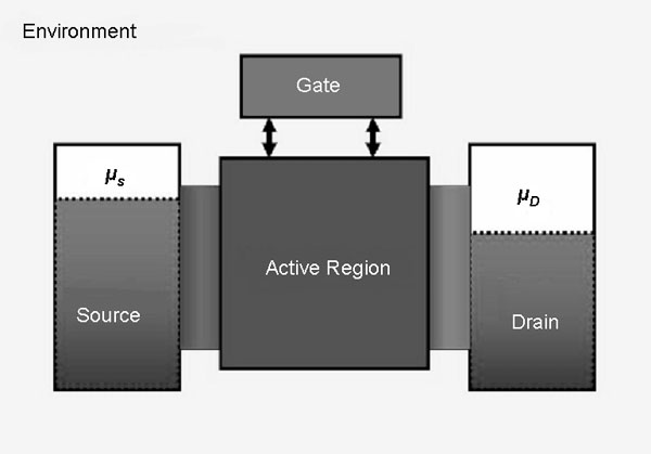
The ‘device’ is coupled to two contacts, left and right, which serve as a source and sink (drain) for electrons. Here the contacts are drawn as metallic-like reservoirs, characterized by chemical potentials μs and μD, and are separated by an external bias, qVA=μs - μD. The current flowing through the device is then a property of the chemical potential difference and the transmission properties of the active region itself. A separate gate electrode serves to change the transmission properties of the active region, and hence modulates the current. This separation of a nanodevice into ideal injecting and extracting contacts, and an active region which limits the transport of charge, is a common way of visualizing the transport properties of nanoscale systems. However, it clearly has limitations, the contacts themselves are really part of the active system, and are driven out of equilibrium due to current flow, as well as coupling strongly to the active region through the long range Coulomb interaction of charge carriers.
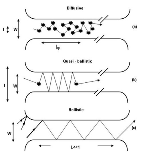
The nature of transport in a nanodevice such as that illustrated above, depends on the characteristic length scales of the active region of the device, L. The figure below illustrates the active region of this nanodevice in terms of a conductor of length L, and width W. The mean free path between collisions is designated l, while the length scale over which quantum coherence is preserved (the phase breaking length), is designated lφ. The latter is often associated coupling to the environment is associated with quantum mechanical phase breaking. Figure a) corresponds to the case in which both L and W are much larger than both the elastic and inelastic mean free paths.
Here transport is purely diffusive, and the system behaves essentially as a semi-classical metal or semiconductor governed by the BTE. In Figure b), the width, W, is smaller than the characteristic mean free path, while the length, L, is still much longer. This regime corresponds to the case of a quantum confined system, in which the motion of carriers is quantized in one dimension, but essentially behaves as a diffusive conductor in the other directions. Quasi-two-dimensional and quasi-one-dimensional systems correspond to this case. Finally, when both L and W are shorter than the elastic and inelastic mean free paths, the system is purely ballistic, and the motion of charge is governed by the wave-like behavior of the particle and its reflection and transmission properties through the structure.
Acknowledgement

This web page is an excerpt from the chapter "Transport in Nanostructures" by Stephen Goodnick in the book Nanoelectronics and Photonics: From Atoms to Materials, Devices and Architectures (with permission from the author and the Springer).