|
NGC2007 Satellite Workshop: Materials in Action
In-situ Observation of Nanometer Scale Physical and Chemical Reaction of Materials
Satellite Lecture and Hands-OnWorkshop
Thursday March 15, 2007, 3:30PM
|
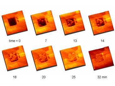
SPM has a unique ability to observe in-situ nanometer scale physical and chemical reactions under a very wide range of sample temperature, atmosphere exposure, fluid immersion, voltage and potential control, magnetic field and other mechanical stress exposure of the sample.
The presentation will include the physics of SPM, followed by the discussion of in-situ SPM measurement of samples under controlled environment.
|
The following topics will be included in the discussion:

1.	How to choose an imaging mode, imaging media and probes to study morphology, softness, conductivity and surface energy
2.	How humidity influences SPM imaging quality in both topography and conductive mapping
3.	How to understand phase imaging of soft samples
4.	Using high / low temperature control, humidity control, organic vapor exposure and fluid treatment study polymer morphology
             change for ultra-thin polymer films
5.	Voltage and potential induced stress, defect formation and cracking of metal thin films studied using EC-AFM
6.	Mechanical property studies at nanometer scale resolution
7.	Data analysis and rendering
|
Following the lecture we will conduct a hands-on session in the ASU
Scanning Probe Microscope laboratories.
We invite you to bring samples.
Please contact Joan_Horwitz@agilent.com (Tel: 1-480-756-5905) for further information.
|
|